For once, nature works in our favour in the fabrication of the necessary
structures on the silicon wafer faces.
First experiments indicate that a (100) surface wafer can be relatively easily
preferentially etched to give the required (111) pyramids, and use of an
infrared mask aligner makes it possible to align hill and pit masks on opposite
faces in the usual manner.
The incident angle of the incoming infrared pixel beams on the pyramid facets
(![]() ) is determined by the cubic crystal structure of silicon.
The refractive index (3.4929 for a wavelength of
) is determined by the cubic crystal structure of silicon.
The refractive index (3.4929 for a wavelength of
![]() [2, page 641,]) and the thickness T
(
[2, page 641,]) and the thickness T
(![]() ) of the parallel polished wafer define of themselves the
lateral dimension W (
) of the parallel polished wafer define of themselves the
lateral dimension W (![]() ) of the pyramids if the correct
straight-through relation between the input and output optical paths is to be
maintained (figure 16).
For pixels of this size we can neglect problems caused by diffraction at the
facets, but to make a practically useable component anti-reflection coatings
would be necessary to boost the total transmission through the structure.
) of the pyramids if the correct
straight-through relation between the input and output optical paths is to be
maintained (figure 16).
For pixels of this size we can neglect problems caused by diffraction at the
facets, but to make a practically useable component anti-reflection coatings
would be necessary to boost the total transmission through the structure.
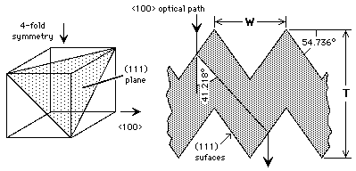
Figure 16: Relationship between crystal directions and the (111) pyramid facets,
and a cross-section of the required silicon wafer
The wafer surfaces are first covered with a 10 micron ![]() film, grown
by wet oxidation at
film, grown
by wet oxidation at ![]() for 1 hour.
This is masked and locally etched away with
for 1 hour.
This is masked and locally etched away with ![]() to define
the regions where the silicon is to be later removed.
The
to define
the regions where the silicon is to be later removed.
The ![]() etching for the pit side requires a mask consisting of a
pattern of crossed lines, which then make up the unetched regions in the
resulting design, and the hill side mask is a square pattern of points,
modified to take account of subsidiary directional etch distortions and
under-etching.
The silicon itself is etched with 0.78 mole KOH at
etching for the pit side requires a mask consisting of a
pattern of crossed lines, which then make up the unetched regions in the
resulting design, and the hill side mask is a square pattern of points,
modified to take account of subsidiary directional etch distortions and
under-etching.
The silicon itself is etched with 0.78 mole KOH at ![]() for 56
minutes [3], which corresponds to an etching rate of about 2
microns/minute.
for 56
minutes [3], which corresponds to an etching rate of about 2
microns/minute.
Etching results correspond well with the originally proposed design, as can be seen from the SEM photograph of a pit-etched side in figure 17.
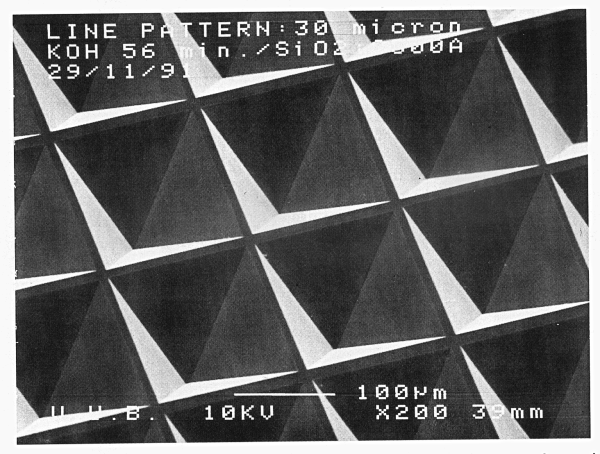
Figure 17: SEM photograph of one side of the wafer, showing the regular array of
pyramid pits